
PRODUCTS / COMPONENTS / FILTERS /
Highpass RF Filters
Low insertion loss highpass filters (0.1 dB) are essential for many of today’s defense platforms and modern wireless environments that require spectral fidelity. Low insertion loss highpass filters (0.1 dB) help receivers to detect and process low power targets as well as discern targets of interest in an interference heavy landscape. Spectrum Control offers 0.1 dB loss highpass filters to both help identify weak communication transmissions as well as recognize valuable intelligence signals in a crowded spectrum.
Visit our Highpass Filter Customization Tool today to optimize your demanding filter requirements.
Our database of low loss highpass filter designs (0.1 dB) helps eliminate the need for additional gain when size, weight and power (SWAP) initiatives are in place. Low loss highpass filters from Spectrum Control also help suppress harmonics on a receiver front end when complex pulse or chirp signals are cascaded on a receive side chain. Also critical where flat amplitude response in the chain can help prevent distortion and unwanted spurious modulation.
Spectrum Control’s line of low loss highpass filter designs (0.1 dB) offers low insertion loss as low as 0.1 dB all while optimizing pole placement strategies to reach the highest rejection in a compact design. These High-Q highpass filters (insertion loss 0.1 dB) can also help maintain receiver sensitivity in a crowded wireless spectrum. High insertion loss from other manufacturers, can lead to excessive heat which then requires additional cooling strategies, or unwanted heavier metal packaging to eliminate thermal runaway.
Low-loss highpass filters (0.1 dB) from Spectrum Control improve signal-to-noise ratio (SNR) performance by providing a lower-loss path for weak signals, maintaining spectral purity without harmful bit-error-rate (BER) degradation. Spectrum Control also offers Rapid Filter options, providing highpass filters in both Chebyshev and Elliptic responses to meet critical demand requirements.
Visit our Highpass Filter Customization Tool to help optimize your demanding filter requirement today.

Highpass filter frequency response
Lumped Element Highpass Filters
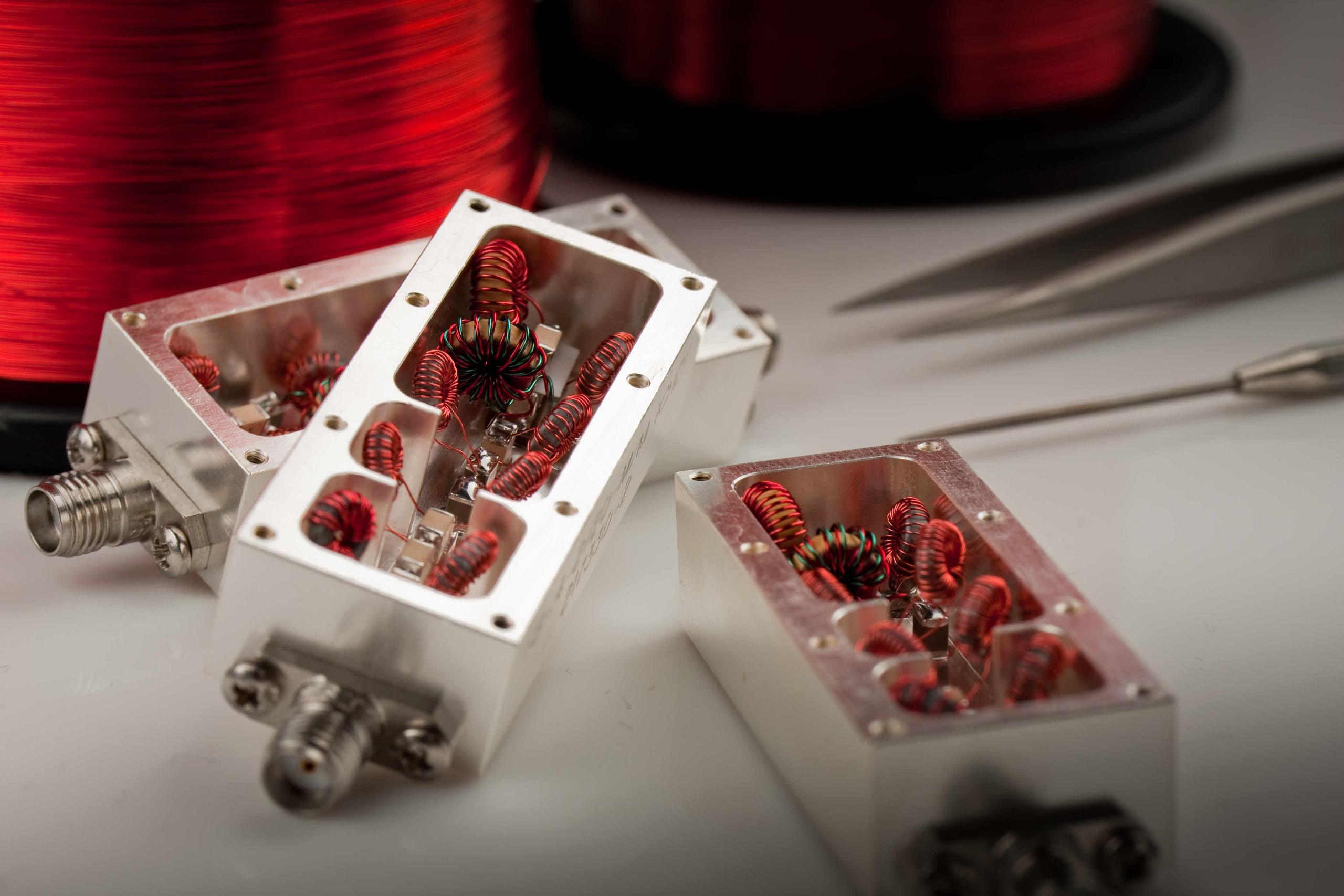
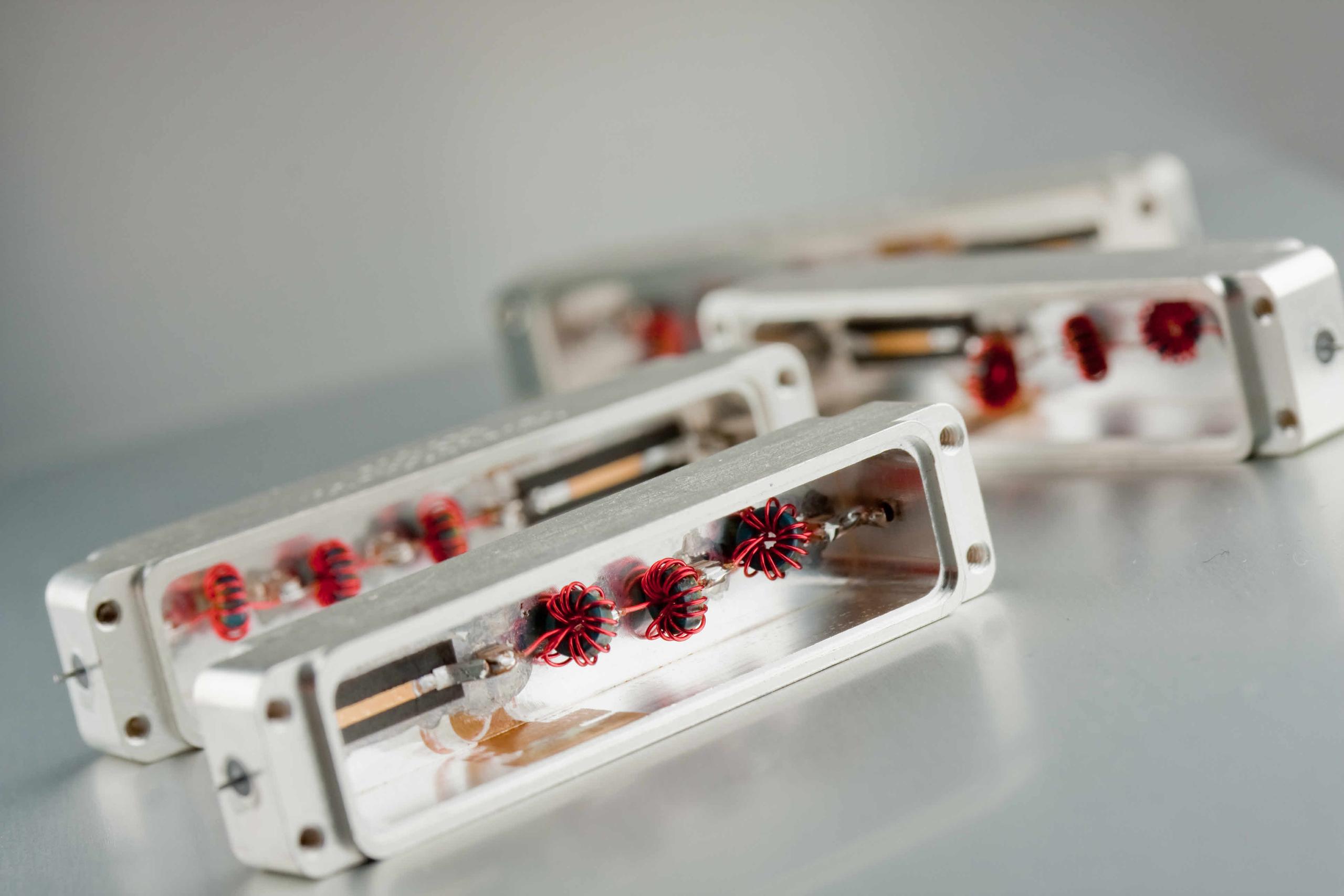
Spectrum Control’s superior low-loss (0.1 dB) lumped element designs are ideal for applications where size and weight are critical. Our filter engineers are experts in lumped element design techniques and employ a range of innovative methods to meet today’s demanding specifications.
- Lightweight surface-mount packages for airborne applications
- Silver plating to reduce insertion loss
- Integral shielding for improved isolation
- Strategically placed poles for maximum rejection
- Multiple topologies integrated within a single package for broad frequency coverage
Spectrum Control’s lumped element filters are designed using discrete inductors and capacitors, covering HF, VHF, UHF, L-band, and portions of S-band (approximately 10 MHz to 3000 MHz). Below 1000 MHz, wavelengths are relatively long; distributed-element filters like cavity filters must be at least a fraction of the operating wavelength, which can make cavities physically larger than other topologies such as lumped elements.
Because discrete capacitors and inductors are much smaller than the operating wavelength, lumped element filters can achieve a smaller footprint than cavity designs.
Distributed-element filters, such as cavity filters, can exhibit spurious passbands, harmonic passbands, or a re-entrant response because their performance depends on the physical dimensions of the structure relative to the wavelength.
By contrast, Spectrum Control’s lumped element filters are smaller than the operating wavelength and therefore do not exhibit re-entrant modes or undesirable harmonic passbands, resulting in a cleaner response. They can also achieve very wide fractional bandwidths (roughly 10% to 90%), which can be difficult to replicate with narrow-band cavity-style topologies.
Lumped element filters are relatively easy to tune by adjusting poles using air-spaced inductive coils. Because these designs typically use standard, off-the-shelf discrete elements and don’t require complex specialized machining (unlike cavity filters), they generally offer lower cost and high customizability.
3D Glass Highpass Filter
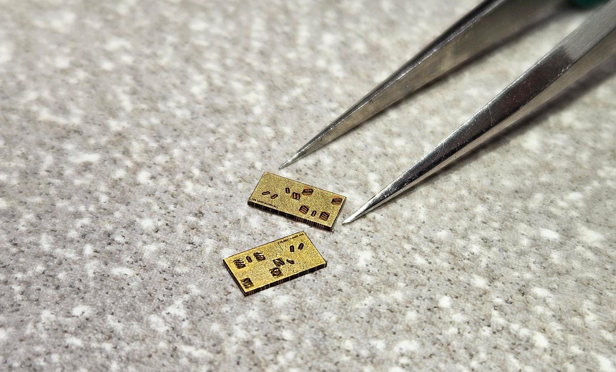
Spectrum Control continues to advance filter technology with the release of its new ultra-miniature glass filters. These high-Q filters, operating at frequencies up to 10 GHz, offer a range of outstanding features, including:
- Low insertion loss below 2 dB in many designs
- Rejection levels up to 70 dB
- Group delay of 1 ns across temperature
- Input power handling up to 1 watt
- Customization to meet demanding requirements
Suspended Substrate Highpass Filters
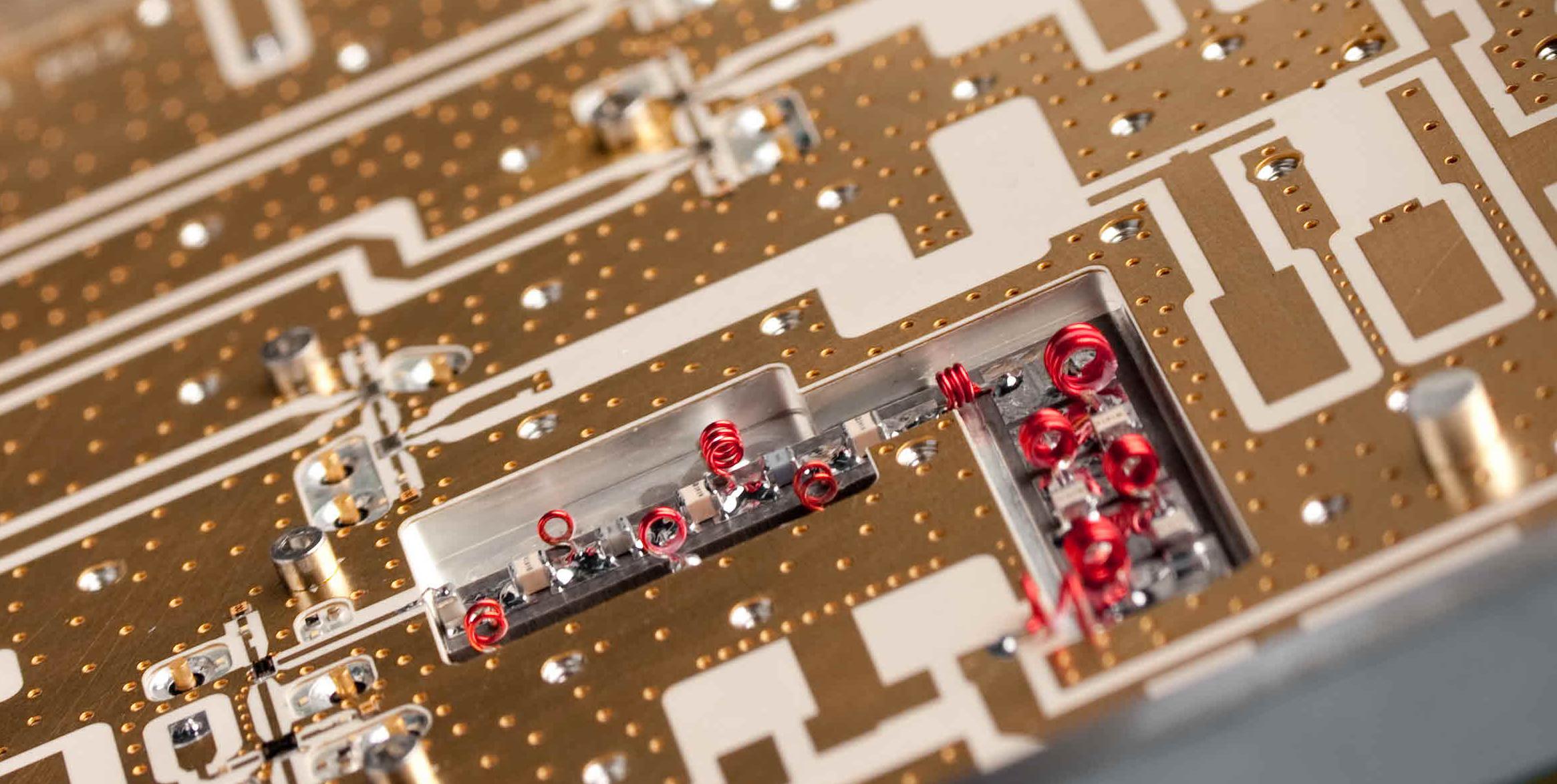
Spectrum’s low-loss suspended substrate filters enable complex transfer functions by integrating multiple filter topologies within a single package. Spectrum Control’s expert engineers optimize low-loss suspended substrate designs to meet demanding performance requirements. Suspended substrate features include:
- Expertise in combining lumped and distributed elements within a single suspended substrate design, providing enhanced unloaded Q and exceptionally low insertion loss
- Gold vias for superior isolation
- Cauer pole–placed transfer functions that yield low insertion loss performance
- Integrated cleanup low-pass filters for improved broadband performance
Butterworth vs. Chebyshev vs. Elliptic
When selecting the optimal shape factor for an RF filter, one must consider the trade-offs between different topologies. One must consider the platform or application as leading elements in the decision to steer the design from one topology to another. For most general RF filter requirements, shape factors are paramount; but one must consider Group Delay Variations, Passband Ripple, Transition, Loss, and other elements that could affect the RF Chain after the filter passes the receive-side waveform.
RF filter design firms like Spectrum Control, select from four main transfer functions when responding to application specific requests. A Butterworth function appeals to requirements for a maximally flat passband. To achieve this, poles in a Butterworth function are arranged and distributed in an evenly symmetric pattern for maximum flat amplitude. This ripple free design does have other consequences; it generates a more gradual transition into the stopband.

Now looking “top down” at both a 5 pole Butterworth and a 5 pole Chebyshev, they both visually look the same. Both functions consist of a normal ladder configuration, series inductor, shunt capacitor, series inductor, etc. However, with a Butterworth function, resonators offer smooth loading with evenly placed values. No resonator value dominates the circuit.
Coupling coefficients and energy distribution are uniform across the network. In a moderate 5-pole Butterworth, adjusting the load on one resonator, the effect is localized and doesn’t wildly disturb the effect of other neighboring sections. No one resonator dominates the circuit. Even though the center element in a Butterworth function is the largest, compared to a Chebyshev function, the center element is not as inflated.
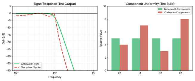
For ultra flat passband response, a Butterworth function prevails. A Butterworth function has a gradual transition, and offers flat passband response. Waveform distortion is minimized which makes it ideal for radar applications, targeting platforms and Electronically steered active array antenna systems.

If, however, the goal is minimizing group delay variation and phase deviation, then the natural selection of functions would be a Bessel function. Bessel function poles are positioned to minimize group delay variations over the passband. Looking at a typical Bessel function passband, as the passband signal approaches the cutoff frequency, the filter circuit comes into view. The capacitors and inductors come to life, storing and releasing RF energy; phase shift increases near cutoff due to reactive energy storage. This storing and releasing effect takes a little time. Over time, the phase of the incident waveform begins to bend. With Bessel function, the phase is uniform, in much the same way a well-engineered highway bends; the lanes are banked slightly so vehicles on each other’s side curve at the same rate and exit side by side as they entered.
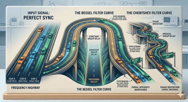
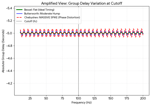
Compared to a Chebyshev, however, where sharp rejection is paramount, the curve is erratic, the bend is sharp and the lanes aren’t uniform and synchronized. Cars (like signals) exit the curve at different rates, no longer side by side, analogous to Phase Distortion.
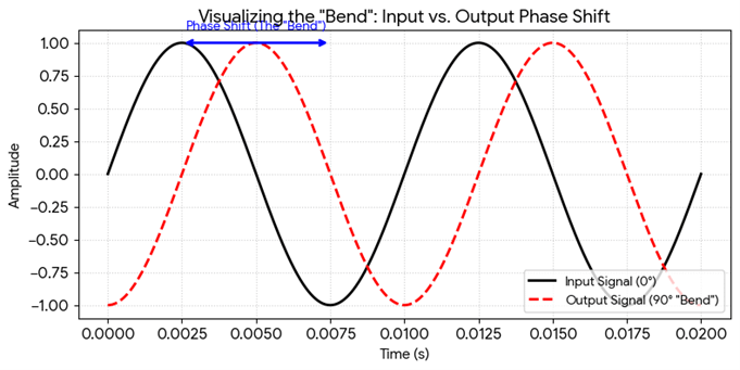
With a Bessel function however, you retain phase linearity but give up rejection. In the design, very specific non-uniform component values are incorporated to achieve that flat phase response. At the cutoff transition, the passband presents a rounder knee, and doesn’t offer as much protection against frequencies on either side of the stop and stop band.
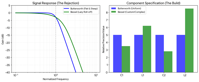
When focusing on maximizing steep skirts, maximum rejection and sharp roll-off, a Chebyshev function is preferred. A Chebyshev shape factor is much more pronounced than a Butterworth or a Bessel function. Passband ripple is more pronounced as the poles are distributed nearer the cutoff frequency. This however has an adverse effect to phase variations. Signals near the passband edges will be delayed more so than signals in the center of the passband affecting group delay. This function is highly non-linear, with reduced pulse fidelity, causing ringing and timing distortion. A Chebyshev exhibits a higher degree of passband ripple coupled with a rapid slope change. However, when steep rejection is required, a Chebyshev function often prevails.
The last of the core filter transfer functions, where sharp roll-off is required centers on an Elliptic (or Cauer) function. An elliptic offers a steep brick wall passband profile with a sharp shape factor and excellent selectivity. Elliptic functions have both passband and stopband ripple. Because an elliptic function requires high selectivity, poles tend to be crowded near the passband transition while transmission zeros are strategically placed in the stopband. Elliptic filters introduce finite-frequency transmission zeros, enabling extremely sharp rejection for a given order. This function also possesses a higher degree of complexity over other filter functions. A Cauer’s phase response is inherently non-linear and probably not a good candidate for applications where group delay variations can affect the RF Chain and system level performance.
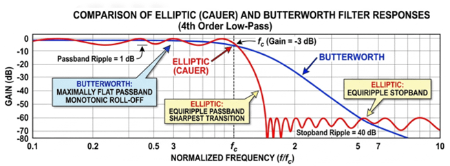
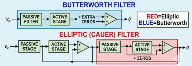
Because steep rejection is paramount, phase linearity suffers the most. Group delay deviations increase significantly as the signal enters the band edges. For Phased Array Radar applications, this inherent phase distortion and group delay spiking makes Cauer functions not good candidates for time domain based platforms.
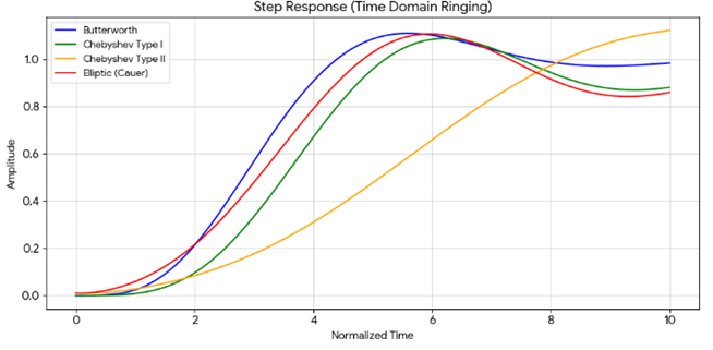
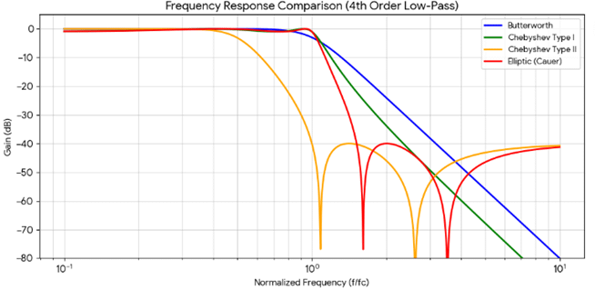
In conclusion, when selecting filter functions, selectivity, Insertion Loss, or rejection should not be the only elements to consider. Group Delay Variations or Phase Deviation at times can play an equal role in deciding filter functions based on intended platform application.
RF Filter Selectivity vs. Insertion Loss
In RF design, two key parameters, selectivity and insertion loss, are inherently opposed. Improving close-in rejection almost always results in increased insertion loss.
Selectivity defines how sharply a filter transitions between the passband and stopband while rejecting nearby unwanted frequencies. To achieve a steeper skirt, RF filter designers often add additional sections to the design.
Adding sections increases the attenuation rate on either side of the transition band. For example, in a Butterworth topology, each pole adds roughly 6 dB per octave (20 dB per decade) of rejection. Higher-order filters sharpen the passband, improving isolation and enabling detection of receive-side signals near or below the noise floor.
There is a trade-off when adding poles: insertion loss becomes more significant. Increasing selectivity by adding reactive elements (i.e., capacitors and inductors) introduces additional loss, as all components have finite Q and inherent resistance. Each added pole in the RF filter design improves selectivity and rejection but also increases signal loss as it passes through these elements.
Impact of Per-Pole Loss: 3-Pole vs. 7-Pole

Higher-order designs with six or seven sections are more sensitive to component tolerances and layout parasitics than lower-order designs. Small impedance mismatches between poles can create reflections, resulting in insertion loss and passband ripple. As more sections are added to achieve sharper rejection, precise tuning becomes critical.
Because each section’s impedance depends on adjacent sections, small mismatches can degrade alignment. In a modest three-pole design, 5% mismatches may be insignificant. In six-pole or higher designs, however, smooth transitions break down, and reflections from mismatches can redirect power back toward the source instead of to the output. Higher-order designs, such as Chebyshev topologies, require tight tolerance control of each element.
If a capacitor deviates from its expected value due to temperature variation or tolerance, the flat passband can develop ripple. Moreover, high-frequency parasitics (e.g., substrate effects, trace lengths) can shift the center frequency, creating challenges in identifying compromised components within the RF chain.
Effect of Filter Order (Poles) on Rejection & Roll-off

Even small mismatches between poles, such as impedance variations from 47 to 53 ohms across the band, can generate reflections toward the source. Adding more poles increases this effect and degrades return loss. Losing even 5% of incident power can create standing waves and passband ripple through constructive and destructive interference. Dissipated power becomes heat within the resonator structure, further amplifying thermally induced variations.
Different filter designs prioritize parameters differently. Butterworth topologies typically offer lower insertion loss and a flat passband but less selectivity. Chebyshev topologies provide sharper skirts but introduce passband ripple. Elliptic topologies deliver the highest rejection but can produce ripple in both the passband and stopband.
Magnitude Response: 7-Pole Highpass Comparison

Why Group Delay Matters in RF Filter Design
Group delay is critical because it determines the timing, period, and phase accuracy of incident signals and waveforms. While an RF highpass filter is primarily designed to select the operational band and pass only the desired portion of a waveform, it must also preserve waveform integrity. To maintain spectral purity, all elements in the RF chain should exhibit consistent time delay, or a linear phase response. If a highpass filter does not adequately control group delay, signals can disperse or distort, compromising downstream performance.
Distorted pulses may overlap, making it difficult for receivers to separate and analyze individual signals. Variations in group delay can cause widening, spreading, or blending of signals, particularly when multiple channels experience differing phase responses. This can lead to inaccurate measurements, degraded analysis, and increased bit error rates, making it harder to distinguish where one data packet ends and another begins. When signals reach the analog-to-digital converter, this distortion can impair accurate edge detection and signal interpretation.
In radar systems, precise timing is essential for accurate distance measurement. Group delay variation can distort pulses and reduce waveform fidelity. In modern phased-array radar systems, phase is used to steer beams, making flat group delay critical for accurate targeting and frequency tracking. While high-Q, high-selectivity filters are often preferred, designs such as Chebyshev filters can introduce greater group delay variation near the 3 dB points. In contrast, Bessel filters provide the flattest group delay response among common filter types, making them ideal for applications requiring minimal waveform distortion.
Relationship Between Phase and Temperature in RF Filters
High-Q RF filters, such as ceramic and low-loss cavity designs, are sensitive to temperature variations and often require thermal conditioning to maintain stability under all conditions. These filters are frequently used in group-delay-sensitive, phase-critical RF chains where phase linearity is essential (Low Phase Noise Amplifiers, Spectrum Control).
When used in the same RF chain as a low phase-noise amplifier, the entire RF cascade becomes phase-centric, as seen in receive-side radar applications or quantum computing platforms. In these cases, precise timing of the modulated waveform is critical to overall system performance.
As a highpass filter heats up, due to input power dissipation or environmental conditions, the physical structure of its elements can change, along with the values of capacitors and inductors. When a lumped-element filter absorbs incident RF power, capacitor characteristics can shift and inductor dimensions can change, affecting overall performance.
Inductors generally experience temperature-induced parameter drift (ppm/°C) as their materials heat up. In ferrite-core inductors, changes in permeability can shift inductance and reduce Q factor, while in air-wound inductors, heating of the conductor can also affect performance. As a result, temperature variations can alter inductance values and degrade overall filter performance.
Initial Permeability (µi) vs. Temperature

Capacitors are also susceptible to temperature drift (ppm/°C). At higher temperatures, thermal energy causes molecular motion within the ceramic structure. In materials such as barium- or tantalum-based dielectrics, the crystalline structure includes displaced central atoms, making the capacitance sensitive to temperature changes.
As temperature changes, domain alignment within the crystal structure shifts, altering the dielectric constant. This results in capacitance drift, which can impact insertion loss and phase linearity.
Capacitance Change vs. Temperature (Tantalum)

Because phase response depends on temperature-sensitive material properties and design techniques, temperature variations can increase an RF filter’s susceptibility to phase distortion and group delay ripple across frequency and operating conditions.
These changes can distort signal fidelity in systems where flat group delay is critical, such as phased-array antennas and radar. Temperature-induced group delay variation can cause phase divergence, leading to beam-pointing errors (beam squint) in wideband applications.
Technical Questions
Why is my filter’s measured return loss or VSWR worse than the filter datasheet or specification?
When troubleshooting measurements that don’t match a manufacturer’s datasheet, a common issue is calibrating at the VNA port instead of at the cable termination. Calibrating at the port includes cable loss and mismatch in the measurement. To ensure accuracy, gently flex cables before calibration, not after, to minimize amplitude and phase drift.

Why is the measured insertion loss higher than the simulated model?
When using ADS or Genesys, ideal component values with infinite Q are typically assumed by default. In practice, real components have finite Q and non-ideal characteristics. Factors such as FR4 substrates, trace widths, pad inductance, and connector interfaces can shift center frequency and add several dB of insertion loss.

Why does the datasheet or spec sheet for my highpass filter specify 1.2:1, but I’m measuring 1.8:1?
The BPF datasheet was likely measured using low-loss SMA connectors or mates closely matched to 50 ohms, resulting in minimal reflection at the input. At frequencies above 1 GHz, impedance mismatches become increasingly critical to VSWR measurements. Open-channel designs, where nearby active signals create antenna-like effects, can also increase VSWR. Additionally, if the BPF is mounted on standard FR4 while the manufacturer’s test fixture uses a material like Rogers 4350B, impedance differences in the traces can lead to degraded VSWR performance.

How do I optimize the microstrip to highpass filter transition on my board?
First, narrow the pads. The transition is likely wider than the 50-ohm microstrip leading to the pad, creating parasitics and reflections. When adding vias, increase the number of ground vias near the pads and place them directly under the filter to reduce inductance as the return path seeks ground.

Do I have enough grounding vias near my highpass filter inputs and outputs?
If your BPF includes shunt capacitors, a copper-filled via can behave like a small inductor as the signal seeks a ground path, especially if the via is not placed directly under the filter or as the signal transitions through it, thereby increasing S11. Poorly placed grounds introduce inductance, and longer return paths increase characteristic impedance, further degrading S11.
