Space Qualified Amplifiers
Can't find the RF amplifier you are looking for?
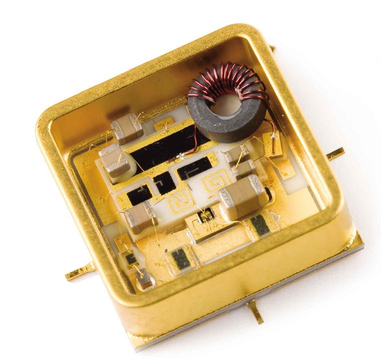
What is a Chip and Wire Amplifier?
Advantages of Chip-and-Wire Amplifiers over MMIC Designs for RF Applications
Executive Summary
Selecting the optimal amplifier technology has a significant impact on RF system performance in communications, radar, aerospace, and instrumentation applications. This white paper compares traditional chip-and-wire amplifier assemblies with monolithic microwave integrated circuit (MMIC) designs, highlighting their distinct performance advantages in critical areas, such as low noise amplifiers (LNAs), ultra-low phase noise amplifiers, and high-linearity amplifiers and supports these findings with real-world examples and quantitative data.
Introduction
The choice of amplifier technology can significantly affect system effectiveness, reliability, and longevity. While MMIC amplifiers are widely adopted for standardized, high-volume applications, chip-and-wire amplifier assemblies deliver unmatched customization and superior performance. Advantages that are especially valuable in specialized or performance-critical RF systems.
Key Performance Advantages
1. Superior Low-Noise Amplifier (LNA) Performance: Chip-and-wire amplifier assemblies give engineers the flexibility to select discrete transistors and precisely matched passive components, explicitly optimized for minimal noise figures. With careful hand-selection and meticulous tuning, these assemblies consistently achieve lower noise figures than typical MMIC counterparts. This translates directly into enhanced sensitivity and improved system-level performance, especially in radar and communication systems.
Example: A radar system using chip-and-wire technology achieved a lower noise figure of just 1.2 dB over a narrower targeted bandwidth. In contrast, a comparable MMIC solution delivered 2.1 dB but was designed for a much broader bandwidth, sacrificing noise figure for coverage. The lower NF of the chip-and-wire approach translated into a dramatically enhanced target detection range.
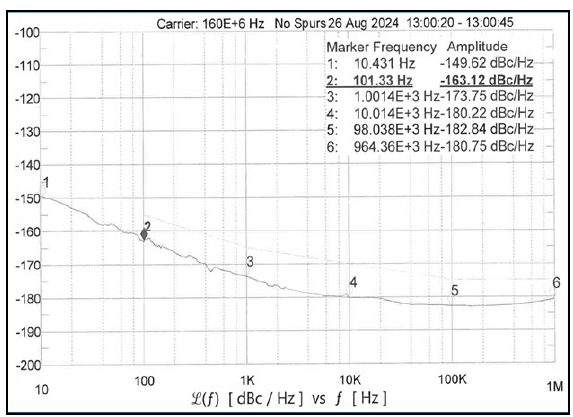
2. Exceptional Ultra-Low Phase Noise Amplifiers: In applications demanding precise signal integrity, such as high-frequency defense targeting and advanced radar systems, chip-and-wire solutions often outperform their MMIC counterparts. Their discrete construction enables fine-tuned optimization of both transistor selection and circuit layout, significantly reducing residual and additive phase noise across the RF chain.
Example: Testing has shown that chip-and-wire designs deliver residual phase noise improvements of up to 10 dBc/Hz (at a 10 kHz offset) compared to similar MMIC designs.
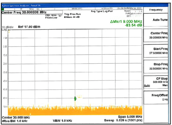
3. Enhanced High Linearity Amplifiers: Depending on the high linearity performance requirements, second-order harmonic behavior may provide distinct advantages over third-order two-tone levels, particularly when suppression of even-order harmonics is critical. Ultra-high linearity chip-and-wire amplifier designs often employ multiple push pull and Darlington circuits to cancel these harmonics, delivering effective out-of-band harmonic filtering. This prevents unwanted harmonic energy from crowding the fundamental and generating in-band spurious signals.
Example: A major defense contractor upgrading an over-the-horizon threat detection radar required IP2 performance levels not typically achievable with traditional MMIC designs. A standard 16-transistor hybrid chip-and-wire design delivered +100 dBm (IP2 two-tone), enabling the team to eliminate additional filters previously needed to suppress even order harmonics.
Free Modifications to Standard Amplifiers
Modern chip-and-wire amplifier circuits deliver inherent advantages through their extensive customization potential. Unlike MMIC amplifiers, where integration can restrict optimization, chip-and-wire amplifier designs provide unmatched adaptability, enabling engineers to fine-tune every parameter to exact system requirements. This flexibility ensures maximum compatibility and improved performance across a wide range of RF systems and applications.
Example:
Reliability and Thermal Management
Chip-and-wire amplifiers inherently deliver superior thermal management, thanks to precise component-to-package placement and advanced surface-mount engineering. This improved heat dissipation leads to higher mean time between failures (MTBF), a critical advantage in demanding aerospace and defense applications.
Cost-Benefit Analysis
While MMIC designs may appear on the surface to be economically attractive initially for high-volume standard applications, chip-and-wire amplifiers deliver enhanced performance and reliability over time. Their superior operational lifetime, reduced maintenance requirements, and improved performance metrics often offset initial investment differences, proving highly cost-effective in specialized markets such as defense, aerospace, and critical communication infrastructures.
Conclusion
Chip-and-wire amplifier assemblies consistently outperform MMIC designs in key areas, including low noise, ultra-low phase noise, and high linearity. With the ability to be precisely optimized and engineered for superior reliability, chip-and-wire technology stands out as the clear choice for high-performance RF amplifier applications.
Download the PDF: Advantages of Chip-and-Wire Amplifiers over MMIC Designs for RF Applications
How are Gain and Noise Figure Related?
How are gain and noise figure related for low noise RF amplifiers?
In a low-noise amplifier (LNA), gain and noise figure are interrelated but distinct parameters. Generally, they exhibit an inverse relationship, improving one can often degrade the other, depending on the design trade-offs involved. Although gain and noise figure are optimized independently, achieving a high gain in the first stage of an amplifier is particularly beneficial, as it minimizes the contribution of noise from subsequent stages.
How does gain compare to noise figure on a single-stage LNA design?
The noise figure (NF) of an amplifier is defined as the ratio of the input signal-to-noise ratio (SNR) to the output SNR. A lower noise figure indicates better noise performance. One way to reduce NF is by operating the amplifier’s transistors near their maximum current capacity, which increases the signal amplitude relative to the amplifier’s intrinsic noise sources, thereby improving the output SNR.
As amplifier gain increases, both the signal and the internally generated noise are amplified. However, when the gain is sufficiently high, the input noise becomes the dominant contributor to the total noise, effectively reducing the relative impact of the amplifier’s own noise. This behavior is quantified by the Friis formula (or Friis equation), which describes how noise figure accumulates in cascaded amplifier stages.
In practical system design, placing a high-gain, low-noise amplifier (LNA) at the front end, ideally as close as possible to the antenna, significantly minimizes the influence of noise from subsequent stages. For this reason, the first-stage LNA typically has the most stringent noise and gain specifications in the entire receive chain.
Understanding Impedance Matching
Load Termination Requirements
How important is a 50 Ohm termination?
A true 50-ohm termination is critical to the health of a small-signal RF amplifier because it ensures free-flowing signal propagation, maximum power transfer, and prevents damage from output reflections. If a 50-ohm amplifier is placed in an RF chain facing a mismatched impedance, issues, including amplifier failure, may occur. The importance of impedance-matching a 50-ohm small-signal amplifier with surrounding components cannot be overstated; moreover, it is considered an industry standard.
- Maximum Power Output: When the input signal and load impedances are matched to 50 ohms, nearly all of the amplifier’s output power is delivered to the next cascaded chain component. In an unmatched or poorly matched system, some of that power is reflected, either back to the amplifier (when the amplifier sees a mismatch) or back to the source (when the mismatch is at the amplifier’s input).
-
Preventing Signal Reflections: Impedance mismatches cause signal reflections, this is well known. The reflected signal then travels back along the signal path and interferes with the output signal, creating standing (stationary) waves.
-
Signal Integrity: Standing waves can appear as current or voltage fluctuations along the signal path. This can manifest as distortion, a deterioration in the signal-to-noise ratio (SNR), and can seriously affect or degrade the amplifier’s output.
What are the consequences of a mismatch?
When a small-signal RF amplifier operates in a chain with a mismatched impedance, the result can range from a slight reduction in performance to reflections that cause serious or even permanent damage to the amplifier.
Reduced Performance
- Output Power Loss: In a small-signal RF amplifier, any output power reflected from the load is lost energy. This reduces the total power output intended for the downstream component. As the load mismatch worsens, the intended output power loss increases dramatically.
- Distortion: When standing waves are present due to load mismatch, their interference produces distortion, degrading signal fidelity.
- Gain Loss: The gain of an amplifier in an RF chain can be lowered by load-mismatch losses at each gain block stage.
Can impedance mismatches damage an amplifier?
- Transistor Damage: In cases of an open (infinite impedance) or short (zero impedance), all forward-directed output power is reflected back into the amplifier’s output pin or connector. This can cause a sudden and dramatic increase in voltage or current directed at the transistors. Designers sometimes employ diodes to absorb that reflection or large capacitors to ground to drain it away, but such measures are not always 100% effective.
- MTBF: Reflected power must eventually dissipate as heat if the mismatch is severe enough. This additional heat can reduce the mean time between failures (MTBF), shortening the amplifier’s lifespan.
Can I prevent damage to an amplifier which has a poor mismatch?
- Share your Incident Impedance Measurements with the RF Amplifier Supplier: Knowing potential mismatch issues before amplifier selection can help mitigate problems later. Spectrum Control can often include elements such as diodes or pads on the output to help absorb, reflect, or condition harmful mismatch reflections.
- Add a Pad: For reflection-sensitive amplifiers, a small pad, perhaps ¼ dB to ½ dB (if there’s sufficient output power margin), can be strategically placed at the amplifier output or at the next component’s input to reduce reflected power.
- Use Proper Load During the Test Phase of the Design: Always terminate an amplifier with a 50-ohm load. During test sessions, this means using a 50-ohm dummy load. In a system-level evaluation, this requirement extends to the entire RF chain, including connectors, cables, and all other components.
Amplifiers for Critical Space Missions
When selecting an amplifier for a critical Space related mission, one must not only account for the effects of changing conditions related to radiation and temperature swings, but also be aware of which base transistor metallization would be ideal candidates over other base metal transistors and why.
The effects of the space environment on an amplifier vary drastically depending on the orbital regime, mainly due to differences in radiation exposure, thermal extremes, and vacuum conditions. An amplifier on a satellite in low Earth orbit (LEO), medium Earth orbit (MEO), and deep space will face a unique set of challenges that affect its performance and longevity.
Low Earth Orbit (LEO)
LEO is generally between 60 and 1200 miles in altitude. Even though it is in orbit, a LEO satellite is still protected to some extent by the Earth's far-reaching atmosphere. While the earth’s atmosphere as a conventional boundary technically extends out to 62 miles, the atmosphere extends out on a gradually thinning scale to over 300,000 miles (farther than the distance to the moon). At this distance though, it is merely a faint cloud of hydrogen atoms.
Environmental characteristics
- Thermal Cycling: temperature swings from -150°C to +150°C can be experienced by a satellite as it passes in and out of the Earth's shadow. In a LEO orbit, that cycle occurs once every 90 minutes. While Hybrid amplifiers are tested and rated to withstand temperature swings of -55°C to +85°C, without adequate passive heating and ventilation, a low noise amplifier, like any active device, will reach the limits of its own capabilities due to material fatigue, weakening solder joints, and internal bond failures.
- Radiation: LEO satellites are somewhat shielded by the Van Allen belts but must continually contend with solar rays, solar energetic particles (SEPs), and the South Atlantic Anomaly (SAA), a region of weak magnetic field where the radiation belt dips closer to the Earth. Long-term TID exposure can, over time, cause a gradual accumulation of charge in the amplifier's transistors. Without shielding, this can increase leakage currents and voltage shifts, eventually leading to performance degradation. SEEs, or single-event effects, of High-energy particles from solar rays or other solar events can pass through the metal upper assembly cover into the KOVAR amplifier package and strike the amplifier's transistors, causing temporary damage, potential emitter shorts, or single-event latch-ups (SELs).
Medium Earth Orbit (MEO)
A satellite orbiting in a MEO is typically found 1,200 miles to 22,000 miles from Earth, where the most intense parts of the Van Allen radiation belts lie. Because MEO satellites orbit farther from Earth, they tend to experience fewer and shorter eclipses than those in low Earth orbits. There are tradeoffs here, of course; a MEO must endure more consistent solar events than a LEO, but also less frequent and less severe thermal cycling.
Environmental characteristics
- Thermal Cycling: for a satellite in a MEO, the extreme temperature swings can range from roughly -145°C to +60°C; slightly lower maximum temperatures than a LEO due in part to the earth’s reflection contribution in a LEO orbit. Where satellites in a Low Earth Orbit (LEO) experience rapid thermal cycling, of roughly 90 minutes from minimum to maximum, MEO satellites endure slower, but longer exposure to solar thermal stresses due to the average 12-hour orbit cycle.
- Radiation: satellites in a MEO orbit are constantly exposed to the Van Allen belts, which can significantly reduce the transistor’s operational lifespan. This makes a MEO orbit one of the more hazardous radiation environments for a satellite. The constant bombardment by high-energy particles onto a circuit’s transistors significantly increases the probability of damage within the transistor’s metallization layers. To survive an MEO radiation environment, the amplifier’s next-level assembly must be heavily shielded with some form of dense shielding; either Tungsten or Tantalum will generally stop high-energy electrons from penetrating the subassembly.
Deep Space
Deep space refers to regions informally beyond the moon, which puts it at roughly a 250,000-mile starting point.
Environmental characteristics
- Thermal Cycling: with no earth or moon nearby to offer a temperature-stabilizing presence, a deep space satellite will experience extreme temperature differences between its sun-facing side and the backside away from the sun. For example, on a Mars mission, the satellite will be far removed from the sun's benefits and subjected to temperatures of near absolute zero (-271°C).
- Radiation: deep space is constantly permeated by galactic cosmic rays (GCRs), energetic particles from outside the solar system. Unlike Solar Energetic Particles (SEPs) from our sun, GCRs are not related to or tied to our sun’s solar cycles and can penetrate protective shielding. While less frequent than GCRs, solar flares and coronal ejections can release bursts of radiation that can overwhelm some protective measures.
| Environmental Hazard | Low Earth Orbit (LEO) | Medium Earth Orbit (MEO) | Deep Space |
| Primary Radiation | Milder South Atlantic Anomaly (SAA) and occasional solar flares. | Van Allen radiation belts (high proton and electron traffic). | Galactic cosmic rays (GCRs) and unpredictable solar events. |
| Total Ionizing Dosage (TID) | Cumulative dosage is a concern over the duration or term of the mission. | Higher cumulative dosage requires robust radiation countermeasures. | Continuous, low-level cumulative doses from Galactic cosmic rays (GCRs) over a long mission. |
| Single Event Effects (SEE) | Occasional exposure, with added SAA passes. | Frequent, due to constant exposure to energetic particles. | Exposure to High-energy Galactic cosmic rays (GCRs) poses a significant risk if unprotected to transistor damage. |
| Thermal Environment | Frequent and rapid thermal cycling during exposure and non-exposure cycles. | Longer time in direct sunlight, fewer thermal cycles. | Extreme variations between sunlight and deep shadow, with long periods of predicted thermal stress. |
| Reliability Approach | Manageable through component selection and screening. | Demands significant radiation countermeasures. | Requires the highest effort in radiation countermeasures. |
Class A vs. Class AB Operation
Spectrum Control specializes in the design and manufacture of hybrid chip and wire amplifiers. Class A amplifiers differ significantly from their Class AB counterparts. In Class A designs, the devices are biased to conduct current throughout the entire input signal cycle. While this approach delivers exceptional spectral fidelity, it comes at the cost of efficiency, as the amplifier operates at a continuous 100% duty cycle. By contrast, Class AB amplifiers represent a middle ground between Class A and Class B operation. They are biased to conduct for more than half (180°) of the waveform, improving efficiency while reducing the distortion that is typical in pure Class B designs.
|
Performance
|
Class A Amplifier | Class AB Amplifier |
| Heat | Class A amplifiers generate more heat due to their constant DC power consumption and may require a copper bus to dissipate the excess thermal energy. | Class AB amplifiers produce less heat than typical CW Class A designs because their transistors are not continuously operating at 100%. |
| Power | Because Class A amplifiers are less efficient, they generally deliver lower power output compared to Class AB designs. | Class AB amplifiers typically achieve higher output 1 dB compression points due to their more efficient use of the DC supply. |
| Bias | A Class A amplifier conducts DC current throughout the full 360° of signal propagation. The transistors remain in an “always-on” state, even when no RF input signal is applied. | Class AB amplifiers conduct current for more than 180° of the signal cycle. Typical designs employ a push-pull configuration, in which one transistor conducts during the positive half of the waveform while the other transistor conducts during the negative half. |
| Efficiency | Class A amplifiers are inherently inefficient, with typical efficiencies ranging between 20% and 25%. This low efficiency is a direct result of their continuous-wave (CW) operation, which dissipates a large portion of the DC supply power as heat. | Class AB amplifiers are significantly more efficient than Class A designs, with typical efficiencies reaching up to 60%. |
| Fidelity | Class A amplifiers provide the lowest distortion and highest signal fidelity. Since the transistors operate in the linear region at all times, they avoid the “crossover distortion” that can result from clipping or switching transitions. | Class AB amplifiers deliver higher fidelity than pure Class B designs but fall short of the performance achieved by Class A amplifiers. A small overlap is introduced during the conduction phase between transistors, which effectively eliminates the crossover distortion that is characteristic of simple Class B amplifier designs. |
IP3 vs. IP2
RF Amplifier Linearity and Noise
IP3 and IP2 values are measurements of an amplifier’s linearity. They indicate how much non-linear distortion the amplifier produces and how that distortion contributes to the output signal.
Although both IP3 and IP2 quantify distortion, they differ in the type of distortion measured and the impact on overall system performance. In general, higher IP3 or IP2 values correspond to greater linearity and better amplifier performance.
A “linear” amplifier increases the strength of the input signal without altering its original shape. In other words, the output signal is an exact scaled replica of the input. This characteristic is critical in applications that require high spectral fidelity, such as communication systems and precision instrumentation.
To better understand linearity and non-linearity, consider a real-world analogy using a guitar and a frequency generator.
A frequency generator is a highly linear system designed to produce a simple, “pure” tone. Playing a Middle C produces a single sine wave at approximately 261 Hz. In this system, the output amplitude is directly proportional to the input voltage, raising the input simply increases the output level. The resulting waveform is clean and consists of only one frequency.
By contrast, a guitar is inherently non-linear. When a string is plucked to produce Middle C, it does not vibrate solely at its fundamental frequency. Instead, it also generates vibrations at integer multiples of that frequency, known as harmonics. The pluck (input) produces a complex output waveform containing both the fundamental and its harmonics, resulting in a rich and natural tone.
In this analogy, the amplifier’s role is similar to how the intensity of the pluck affects the sound. A harder pluck increases loudness but also changes the harmonic balance, introducing additional distortion. These harmonics, integer multiples of the fundamental, create the overtones that shape the timbre of the sound.
Nonlinearity in the guitar arises from several factors that interact in complex ways: the stiffness of the strings, the material of the body, and the playing technique. Each introduces deviations from ideal harmonic behavior. This nonlinearity makes the guitar sound warm and expressive, whereas the frequency generator produces an artificial, sterile tone.
In amplifiers, similar effects occur. Nonlinearities cause the output signal to deviate from a perfectly scaled version of the input. These distortions can originate from the amplifier’s fundamental design, component quality, or operating environment. When an amplifier operates nonlinearly, frequencies within the input can mix, producing new frequencies that are the sums and differences of the original ones. These intermodulation products are unwanted because they are not harmonically related to the original signal.
No amplifier is perfectly linear, every RF component exhibits some degree of nonlinearity and will eventually reach a point of saturation where the output can no longer increase proportionally with the input. For this reason, linear amplifiers are designed to operate within a specified range where their linearity and thus IP2 and IP3 performance is optimized.
What is an Intercept Point?
-
The intercept point is a mathematical construct used to describe an amplifier’s linearity. It represents the theoretical input power level at which the power of the desired output signal and the power of the distortion products (typically intermodulation products) would be equal.
-
A higher IP2 or IP3 value indicates a more linear device and greater resistance to distortion, meaning the amplifier can handle stronger input signals before nonlinear effects become significant.
-
In practice, amplifiers reach their 1 dB compression point (P1dB) and begin limiting output power well before the intercept point is actually achieved. The intercept point is therefore used as a figure of merit rather than a directly measurable condition.
Why is IP3 more important than IP2?
Third-order distortion products typically appear very close to the fundamental signal frequencies, making them difficult to suppress using standard filtering techniques. These unwanted signals can fall directly within the receiver’s operating band, degrading sensitivity and overall performance.
For this reason, IP3 is often considered the most critical linearity parameter for a receiver. It directly reflects the system’s ability to maintain clean signal integrity and operate effectively in environments with strong, closely spaced signals, such as crowded or high-interference frequency bands.
When is IP2 more important than IP3?
IP2 is generally less critical than IP3 in superheterodyne receivers because second-order distortion products typically fall outside the desired signal band and can be filtered out more easily.
However, IP2 becomes crucial in direct-conversion (zero-IF) receivers, where second-order distortion can create unwanted DC offsets or low-frequency artifacts that directly interfere with the desired signal. In such architectures, maintaining a high IP2 is essential to ensure accurate demodulation and minimize baseband distortion.